The Single-band Transceiver with Low Voltage Power Supply
During QRP expeditions there is a serious concern about the power supply for the equipment. It is not always possible to use large batteries and it would be better to power the radio equipment through common dry batteries, such as the C and D size cells. If the QRP expedition is a long one, the batteries are not likely to last the duration of time needed. Solar batteries often are not adequate to solve the problem of powering the QRP equipment and recharging the batteries.
To help solve this common problem with inadequate battery power, I developed an experimental transceiver that would operate from 3 volts. This transceiver would operate from two dry batteries such as the R20 (C-type batteries). This design enabled operation for up to 10 days operating at 3-4 hours a day. The transceiver operates with extreme reliability all the way down to 2 volts allowing the use of the batteries to a point of near complete discharge. As opposed to buying and using up 10 batteries for a 12-volt transceiver, I found I could get by with only 2 batteries during an expedition.
The above experiment with the transceiver’s power supply showed that with more than 4.5 volts on the final power amplifier caused the output transistor to overheat and fail. However, I found that I could run the transceiver from one or two cells of a lead acid car battery, or two to three nickel cadmium (NiCd) batteries. If such high-capacity NiCd type batteries are used, it will allow operation all summer long.
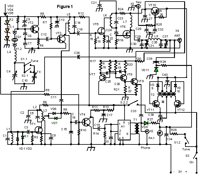
Now, let’s look at the circuit of the transceiver shown below in Figure 1.
Construction for Low Voltage
Operation on the 21 MHz band for multi-station DX contacts was chosen over the other upper ranges (24 and 28 MHz bands) because the propagation on 21 is found to be more stable in comparison to them. Whenever using power as low as 1 watt on this band it is a very reliable band to conduct DX QSO. There are also many amateur stations around the globe using CW on this same 21 MHz band. The transceiver was constructed using a crystal control at one-half the 21 MHz frequency.
It was made this way for the following reasons: Crystals on a 10.5 frequency has enough drive to function as doubler to 21 MHz . By using crystal control, the transceiver is able to operate on voltages as low as 2 volts. Also the transceiver is efficient even with a supply voltage as low as 1.8 volts, but the output power is reduced to 100 milliwatts and the receiver sensitivity drops to 20 microvolts. The mixer stage for reception feeds the frequency twice below 21 MHz range(10.5 MHz). Doing this helps to eliminate image interferencies in RF – preamplifier on VT1 and to eliminate main (bacground) 60 Hz power interference. Thus, the transmit frequency is set at twice the crystal’s fundamental frequency.
Transistor VT2 is the crystal oscillator and it is fed from a stabilized 1.9-volt source. The 1.9-volt source is stabilized by Zener diodes VD3-VD5. C4 allows for a small shift in frequency and, depending on the quartz crystals used, it can be as much as 20 kHz on 21 MHz. Capacitor C10 causes a 800 Hz shift on transmit. For this purpose in the receive mode, with the switch S1 placed in the “set-up” position, the C10 is thus tuned to zero beat with the receiving station.
When in the transmit mode, the transmit frequency will match the frequency of the received station. VT3 is the power amplifier for the heterodyne frequency and this signal is fed to diodes VD6 and VD7. Then the tuned circuit formed by L5 and C14, the high frequency signal then feeds the doubler stage, VT5. In this case two field-effect transistors were used in a bridge configuration. Only one FET is shown in Figure 1 because it is possible to change the circuit and use only one FET with a high amplification factor to allow the transceiver output power of 500-700 milliwatts to be reached.
The power amplifier VT-6 is mounted on a small heat sink made from aluminum measuring 40x40x4 mm. The output tuned circuit is made up of C30, C31, L8, C35 and C37 used in a Pi-network configuration. Since operation is QRP, it is important to keep circuit losses to a minimum, so the tuning capacitors are all air variables. By stretching and compressing L8, then tuning of contour capacitors C31 and C37 with careful selection of capacitors C30 and C35, maximum output power from the transceiver can be obtained.
The final output stage and the doubler are fed from the voltage converter of VT11, VT12. This converter has excellent parameters for usage in QRP gear. Without any load, the current is no more than 10mA. Under heavy load, the efficiency reaches 80%. The converter ensures 20 volts at idle. If the turns are increased in the primary winding, it is possible to increase the output voltage to 25 volts. If this is done, the transmitter becomes very likely to fail and the failure of the final amplifier transistor is most likely if the transmitter is connected to a bad antenna load.
The transformer of the converter is made by winding the turns on a toroidal core with a permeability of 2000 (OD=17, ID=8, H=5mm). The primary winding consists of 80+10+80 turns of a wire with a diameter of 0.12mm. The secondary winding is wound over the primary and consists of 12+12 of a wire with a diameter of 0.5mm. Both windings are distributed evenly over the toroid core. If the transceiver is to be powered at a higher voltage, say from 4.2 to 4.8 volts (voltage generated by three nickel-cadmium batteries or three dry cells), then the number of turns in the primary must be reduced to as much as 48+10+48. This is necessary for reliable operation of the converter.
The converter is turned on when the transceiver is turned on, and even though the current drain is small, about 10mA, it would be desirable to eliminate this drain to increase battery life. So it would become desirable to eliminate VT10 and just use the telegraph key to do the required switching, but this method has problems.
The main problem is that there is a large current to be switched but at a small voltage level. So, when the contacts of the telegraph key make contact there is a large loss of current due to the contact resistance between the two contacts. This makes the use of the switching transistor, VT10 and the switch S2 necessary, to switch the high currents in this circuit.
If after the converter does not work, or the current drain exceeds 10mA with no load, it will be necessary to swap the leads of the secondary winding to get the correct phase shift. When operating correctly, the converter does not cause interference to any received signal. Transistors VT11 and VT12 have screws with 4 nuts inserted in each transistor’s heat sink mounting hole to create the heat sinks. When the transceiver is turned on, the converter is running at all times and the transmitter is keyed by transistor VT10.
The side tone oscillator of 800 Hz generated by VT7-VT9 and is bridged to the RF – power amplifier on VT6 to allow monitoring of the CW transmissions.
VT1 is the RF preamplifier which in turn feeds diodes VD6, VD7 which are the mixers. These stages do not need any alignment (except resonance circuits on L1C1 and L2C5) because the correct voltages are automatically established by the circuits themselves. The only tuning required during operation is to turn the tuning knob and listen for stations to contact.
The preliminary amplifier of a low frequency is made on the transistor VT4. If another transistor with different characteristics is used, it may be necessary to change the value of R9 if it is found that there is inadequate amplification at low frequency.
The base circuit of VT4 feeds from the stabilized voltage from the master oscillator of the transceiver. The optimum amplification of VT4 during my tests was obtained with a collector voltage of 1.8 volts with the power supply using 3vdc.
The final audio stage is a single chip TDA7050. This chip works well at supply voltages ranging from 1.6 to 6 volts. This chip will ensure enough audio output to drive low impedance headphones such as used for a radio or tape player with an impedance of 32 ohms. The small output transformer from an old transistor radio is used to prevent destruction of the audio chip if the headphones should short to ground.
The micro-ampmeter, PA1 came from the audio level indicator of an old tape recorder. It is used as an S-meter on receive and as an output indicator on transmit. This output monitor system is calibrated with a transmitter using a 50-ohm dummy load. When a properly matched antenna of 50-ohms is used, it is then possible to determine when maximum power level is reached. The PA1 is also used to display the battery voltage of the power supply during setup.
| Spools | Inductance Microhenry | Construction |
|---|---|---|
| L1, L2, L6 | 0.7 | Dia: 9mm, Length: 9mm, 7.5 Turns, wire-dia 0.5mm, Ferrite rod for tuning |
| L3 | — | 4 turns on bottom of L2, wire dia: 0.3mm |
| L4 | 10 | Dia: 20mm, length: 20mm, 27 turns, Wire dia: 0.5 mm |
| L5 | 2.4 | Dia” 9mm, length: 9mm, 18 turns, wire dia. 0.44mm, tap at 5th turn. Ferrite rod for tuning |
| L7 | 5 | RF Choke |
| L8 | 0.7 | Dia: 20mm, length: 18mm, 5.5 turns, wire dia: 2mm |
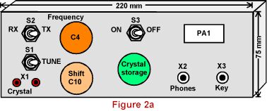
The coil data for the transceiver are listed in Table 1. The transceiver was made from printed circuit boards. The case dimensions are 220x140x75mm. The construction of the transceiver is exhibited in Figure 2a and 2b. The receiver and crystal oscillator are constructed on a separate board and it is mounted on a side of the case. The doubler -power amplifier is constructed on a separate board as is the power converter.
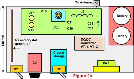
By using this method of construction, the size of the transceiver was reduced. Also it eliminates possible spurious oscillations in the power amplifier and make it easier for the adjustments of the individual circuits. The elements of the power supply consist of two R20 (C size) size batteries which were placed inside the transceiver.
The crystals used had overlapping ranges. These crystals cover part of the phone segment of the band and part of the CW band. They are stored in container made from the 35mm film can. The film can is secured in the transceiver case with scotch tape. It is a good idea for the film can to be taped on all sides to prevent dislodging by accident from the case.
Test Results
The transceiver was tested during the summer of 1999 from the field during a QRP Expedition. A dipole antenna was used and contacts with Western Europe and the Asian part of Russia was easily done. The transceiver had excellent frequency stability, even with changes in temperature and battery discharge. Excellent received signals were reported by the stations contacted.
Characteristics
- Band: 21 MHz
- Mode: CW
- Supply Voltage:2 to 4.5V input
- Receive Current: 40 mA with supply voltage of 3V
- Transmit Current: 800 mA with supply voltage of 3V
- Receive Sensitivity: Not less than 2 microvolts
- Transmitter Output: 500-700 milliwatts
- Antenna for Use with the Transceiver: 30-100 ohm
Transceiver Parts List
| Resisitors |
Capacitors |
|
| R1 100k R2 5k R3 100 R4 360 R5 150 R6 100 R7 5.6k R8 2k R9 360*k R10 51k R11 8k R12 51 R13 8k R14 22k R15 100k R16 220 R17 5k R18 220k R19 220k R20 5k R21 1k R22 1k* R23 100k R24 150 R25 5k R26 2k R27 4*k R28 15*k R29 7*k R30 100 | C1 C2 C3 C4 C5 C6 C7 C8 C9 C10 C11 C12 C13 C14 C15 C16 C17 C18 C19 C20 C21 C22 C23 C24 C25 C26 C27 C28 C29 C30 C31 C32 C33 C34 C35 C36 C37 C38 C39 C40 | 91pFd 0.1mFd 100pFd 10-100pF variable 91pFd 68pFd 150pFd 0.1mFd 0.1mFd 8-30pF variable 0.05 mFd 51pFd 0.1mFd 68pFd 0.05mFd 0,05 mFd 10 mFd/6V electrolytic 200pFd 0.33mFd 3300pFd 0.1mFd 0.1mFd 82pFd 200 pFd 3300pFd 3300pFd 0.1mFd 1mFd 100pFd 110*pFd 8-30pF variable 1mFd 1mFd 1mFd 200pFd 5pFd 8-30pF variable 47mFd/25V electrolytic 5pFd 47mFd/25V electrolytic |
Resistors: All values are in ohms
Capacitors: All are low voltage, 50V will be fine (except electrolytic)
Semiconductor Parts List
- VT11-VT12: hfe=40…70, P=5Wtts,fmax=7 MHz (BD176)
- VT1,VT5: fmax=200MHz, low power (D110-1)
- VT2,VT3,VT7-VT9: silicon low power, hfe=70…100,
P=150Watts, fmax=200MHz (2N3293) - VT4: silicon low power, hfe=1000…1500 (BC123,2N4432A)
- VT10: hfe=40…70, P=5Watts,fmax=7MHz ( BD176)
- VT6: RF-field-transistor for preamplifier
tx and rx, fmax=250MHz, P=2,5Watts ( BFL522) - VD9-VD10: 200V/100mA, 15kHz (1S204)
- VD3-VD5:Zener diodes 0.7V (ZENER DIODE 0.65V)
- VD1,VD2,VD6-VD8,VD11: silicone switching diodes (1N916)
- TDA 7050 audio amplifier or equvalent.
Semiconductors can be substituted as long as they match or exceed the data given here.
Other Parts List
- Audio transformer from transistor radio
- Quartz Jack
- Earphone jack
- Key Jack
- Antenna coaxial cable BNC connector
- Two position toggle switch for set up for transmitting mode
- Two position toggle switch for transmit-receive switching
- Old can from 35mm film
- Power switch
- Battery holder
- Case and PC boards for construction of transmittern
- A microamphermeter from old tape recorder
- A ferrite ring: OD-17mm, ID-8mm, height-5mm, permeability 2000
- Crystals in frequency range 10500-10600kHz
(quartz for common QRP work on 21 MHz, range has frequency 10530 kHz)
Originally posted on the AntennaX Online Magazine by Igor Grigorov, RK3ZK
Last Updated : 31st May 2024