A 100-1000MHz Utility LPDA
In a pair of articles in QEX (“Notes on Standard Design HF LPDAs,” May-August, 2000), I explored some of the problems and pitfalls of designing LPDAs with a wide passband–something of the order of a 10:1 frequency range. The notes focused on antennas for the 3-30 MHz range and ran from 60 to 164 feet long with 20 to 43 elements. Essentially, the bottom line was that if the boom length is too short and if Tau or Sigma–the design constants for an LPDA–are too low, the resulting LPDA will exhibit one or more of the following flaws:
- 1. The overall gain will be too low to be significantly useful.
- 2. The gain will be uneven across the passband, with serious drops in gain at either the low or high end of the passband.
- 3. With increasing frequency, the azimuth patterns will become misshapen relative to the normal or “well-behaved” pattern due to harmonic activity on elements behind the most active element.
- 4. The chance of weakness–frequency regions in which the forward gain deteriorates and even reverses direction due to excessive harmonic activity of elements behind the most active element–increases, if the phase line impedance becomes too low in an effort to increase overall gain.
- 5. The feedpoint impedance will become erratic, with wide excursions of both the resistive and reactive components, so that it may not be possible to yield an SWR under 2:1 for any center impedance value.
Although impractical for amateur installations, the 164′ 26-element model of a standard design LPDA–with slight modifications to even out performance–proved to be among the most promising designs that used the minimum number of elements necessary to suppress nearly all of the difficulties and still yield an average gain of about 7 dBi–about that of a 2-element quad, but spread over a 3+ octave span. Although not perfectly tamed in all respects, the design was deemed at least acceptable.
Interestingly, utility LPDAs are routinely designed for a 10:1 frequency span at VHF-UHF frequencies. Among the common designs are those for 100-1000 MHz. However, in most cases they are short (30-60 inches boom length) and have a low element population (10-14). Such antennas are about half the minimum acceptable size–when rightly scaled–of the HF arrays examined. I have modeled a number of possibilities in the VHF/UHF frequency region, varying the number of elements and the overall boom length in the most common region. All are equally poor performers. 12-element 30″ boom-length LPDAs for the frequency span rarely achieved more than 5 dBi free-space gain–a full dB less than a 2-element Yagi–with ragged and irregularly shaped patterns that emerged at less than half way up the passband. Even longer boom models fail to pass muster with low element densities.
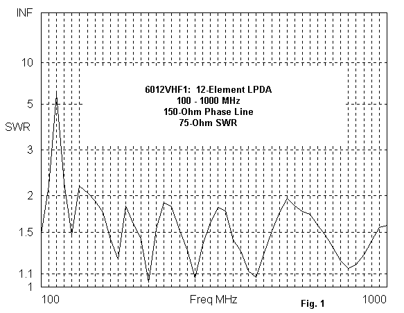
For example, the LPDA whose 75-Ohm SWR curve appears in Figure 1 is designed with a Tau of 0.77 and a Sigma of 0.11 to place 12 elements within a 60″ boom. Once more, irregular pattern shapes emerge very quickly with increasing frequency. Note the spike in the SWR curve. It indicates a potential weakness, that is, a pattern that may even reverse direction.

Figure 2 shows the pattern at 140 MHz. Indeed, it is pointing in the wrong direction due to harmonic activity on elements well to the rear of those which are normally active at the working frequency. The antenna required redesign in an effort to remove the offending anomaly in performance.
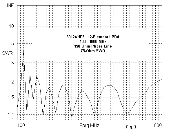
In Figure 3, we have the 75-Ohm SWR curve for one variation on the 60″ 12-element LPDA for 100-1000 MHz. The SWR spike appears to be reduced relative to the one in Figure 1.
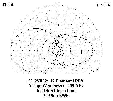
However, the spike is just as great. It has only moved away from the marker frequencies used by the SWR curve (every 20 MHz). The peak anomaly occurs at about 135 MHz, as shown in the free-space azimuth pattern in Figure 4. Once more, the effective beam direction has reversed and the source impedance has reached unusable values.
Satisfactory–if not completely perfect–performance across the 100- 1000 MHz region is more easily achieved if we use more elements, a better choice of Tau and Sigma values, and a sufficiently high phase line impedance. The 164′ 26-element 3-30 MHz HF array used a Tau of 0.9024 and a Sigma of 0.0519. Certain element lengths and spacings–especially at the low end of the spectrum–had been modified for improved low-end performance while retaining good gain at the upper end of the passband.
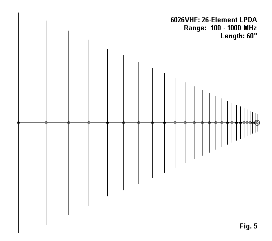
Figure 5 shows the outline of the resulting array. It also shows the outline of the array scaled for use in the 100-1000 MHz range. The most significant changes required in the scaling process were a stepping of the element diameters, with 0.25″ elements used at the low end of the spectrum. The diameter stepped downward in 0.0625″ increments until the most forward and shortest elements used 0.0626″ (about #14 AWG) diameter elements. The overall scaled length is just about 60″. The following table shows the wire set-up for the model.
60″, 26-el 100-1000 MHz LPDA Frequency = 1000 MHz.
Wire Loss: Aluminum — Resistivity = 4E-08 ohm-m, Rel. Perm. = 1
Wires
| Wire | End 1 X (inches) | End 1 Y (inches) | End 1 Z (inches) | End 2 X (inches) | End 2 Y (inches) | End 2 Z (inches) | Diameter (inches) | Segments |
|---|---|---|---|---|---|---|---|---|
| 1 | -29.400 | 0.000 | 0.000 | 29.400 | 0.000 | 0.000 | 2.50E-01 | 107 |
| 2 | -27.210 | 6.969 | 0.000 | 27.210 | 6.969, | 0.000 | 2.50E-01 | 97 |
| 3 | -24.525 | 12.610 | 0.000 | 24.525 | 12.610 | 0.000 | 2.50E-01 | 87 |
| 4 | -22.133 | 17.700 | 0.000 | 22.133 | 17.700 | 0.000 | 2.50E-01 | 79 |
| 5 | -19.675 | 22.293 | 0.000 | 19.675 | 22.293 | 0.000 | 2.50E-01 | 71 |
| 6 | -18.027 | 26.439 | 0.000 | 18.027 | 26.439 | 0.000 | 2.50E-01 | 65 |
| 7 | -16.269 | 30.181 | 0.000 | 16.269 | 30.181 | 0.000 | 2.50E-01 | 57 |
| 8 | -14.683 | 33.557 | 0.000 | 14.683 | 33.557 | 0.000 | 2.50E-01 | 53 |
| 9 | -13.251 | 36.605 | 0.000 | 13.251 | 36.605 | 0.000 | 1.88E-01 | 47 |
| 10 | -11.959 | 39.355 | 0.000 | 11.959 | 39.355 | 0.000 | 1.88E-01 | 43 |
| 11 | -10.793 | 41.837 | 0.000 | 10.793 | 41.837 | 0.000 | 1.88E-01 | 39 |
| 12 | -9.740 | 44.077 | 0.000 | 9.740 | 44.077 | 0.000 | 1.88E-01 | 35 |
| 13 | -8.791 | 46.099 | 0.000 | 8.791 | 46.099 | 0.000 | 1.88E-01 | 31 |
| 14 | -7.933 | 47.924 | 0.000 | 7.933 | 47.924 | 0.000 | 1.88E-01 | 29 |
| 15 | -7.160 | 49.570 | 0.000 | 7.160 | 49.570 | 0.000 | 1.88E-01 | 25 |
| 16 | -6.462 | 51.056 | 0.000 | 6.462 | 51.056 | 0.000 | 1.25E-01 | 23 |
| 17 | -5.832 | 52.397 | 0.000 | 5.832 | 52.397 | 0.000 | 1.25E-01 | 21 |
| 18 | -5.263 | 53.608 | 0.000 | 5.263 | 53.608 | 0.000 | 1.25E-01 | 19 |
| 19 | -4.750 | 54.700 | 0.000 | 4.750 | 54.700 | 0.000 | 1.25E-01 | 17 |
| 20 | -4.287 | 55.686 | 0.000 | 4.287 | 55.686 | 0.000 | 1.25E-01 | 15 |
| 21 | -3.869 | 56.576 | 0.000 | 3.869 | 56.576 | 0.000 | 6.25E-02 | 15 |
| 22 | -3.491 | 57.379 | 0.000 | 3.491 | 57.379 | 0.000 | 6.25E-02 | 13 |
| 23 | -3.151 | 58.103 | 0.000 | 3.151 | 58.103 | 0.000 | 6.25E-02 | 11 |
| 24 | -2.844 | 58.757 | 0.000 | 2.844 | 58.757 | 0.000 | 6.25E-02 | 11 |
| 25 | -2.566 | 59.347 | 0.000 | 2.566 | 59.347 | 0.000 | 6.25E-02 | 9 |
| 26 | -2.316 | 59.880 | 0.000 | 2.316 | 59.880 | 0.000 | 6.25E-02 | 9 |
Sources
| Source | Wire Segments | Wire # | Pct Actual | From End 1 | Specified | Ampl.(V, A) | Phase(Deg.) | Type |
|---|---|---|---|---|---|---|---|---|
| 1 | 5 | 26 | 50.00 | 26 | 50.00 | 1.000 | 0.000 | V |
The actual element lengths are double those shown in the X-column. The element size steps are shown in the second column from the right side of the table. The initial model used a 150-Ohm phase line characteristic impedance throughout. Therefore, that portion of the model table can be omitted in the interests of space.

As shown in Figure 6, the resulting array yields a quite acceptable 75-Ohm SWR curve for the entire passband. The 20-MHz check points on which the curve is based may hide weaknesses. Therefore, suspect regions were checked at closer intervals. For example, the flat peak in the 600 MHz region might hide a high peak between check points. However, it turned out to yield a smooth line when checked at intervals less than 1 MHz apart.
The average free-space gain for the array is just over 7 dBi, with values lower than that at the low end of the pass band and also in the 700 MHz region. The range of gain variation for the array is just over 1 dB. The overlaid free-space azimuth patterns at 100-MHz intervals in Figure 7 demonstrate how consistent the performance is.
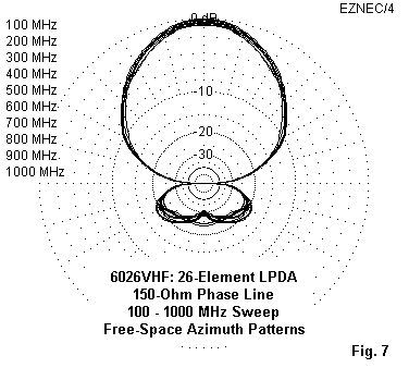
Slight pattern irregularities begin to emerge at about 900 MHz, with a slight “spade” shape to the forward lobe and ripples in the rear lobes. However, by maintaining a 150-Ohm phase line, these affects are minimized while sustaining the highest gain obtainable from the given design.
For some applications, the builder may desire to effect a direct 50-Ohm match for the array. The standard procedure for achieving this goal is to reduce the phase line impedance to 100 Ohms or less. Unfortunately, if the impedance is lowered consistently to this value, weaknesses appear and some patterns display considerable irregularities.
A more modest approach is to use a tapered characteristic impedance for the phase line. If the array were to be constructed using 3/4″ U-channel (2 pieces) for the element supports and phase line, forward channel separation can be closer than the rear separation. Separations of the 3/4″ channel phase lines ranging from about 0.3″ (8 mm) to 0.9″ (23 mm) along the 60″ line length will provide an impedance range of about 75 to 150 Ohms.
The following table shows the simulation of the continuously changing phase line impedance within the model.
Transmission Lines
| Line | Wire # | % Actual | From End 1 | Specified | Wire # | % Actual | From End 1 | Specified | Length | Z0 Ohms | Velocity Factor | Rev/Norm |
|---|---|---|---|---|---|---|---|---|---|---|---|---|
| 1 | 1 | 50.0 | 1 | 50.0 | 2 | 50.0 | 2 | 50.0 | Actual Distance | 152.5 | 1.00 | R |
| 2 | 2 | 50.0 | 2 | 50.0 | 3 | 50.0 | 3 | 50.0 | Actual Distance | 148.0 | 1.00 | R |
| 3 | 3 | 50.0 | 3 | 50.0 | 4 | 50.0 | 4 | 50.0 | Actual Distance | 143.7 | 1.00 | R |
| 4 | 4 | 50.0 | 4 | 50.0 | 5 | 50.0 | 5 | 50.0 | Actual Distance | 139.5 | 1.00 | R |
| 5 | 5 | 50.0 | 5 | 50.0 | 6 | 50.0 | 6 | 50.0 | Actual Distance | 135.5 | 1.00 | R |
| 6 | 6 | 50.0 | 6 | 50.0 | 7 | 50.0 | 7 | 50.0 | Actual Distance | 131.5 | 1.00 | R |
| 7 | 7 | 50.0 | 7 | 50.0 | 8 | 50.0 | 8 | 50.0 | Actual Distance | 127.7 | 1.00 | R |
| 8 | 8 | 50.0 | 8 | 50.0 | 9 | 50.0 | 9 | 50.0 | Actual Distance | 124.0 | 1.00 | R |
| 9 | 9 | 50.0 | 9 | 50.0 | 10 | 50.0 | 10 | 50.0 | Actual Distance | 120.4 | 1.00 | R |
| 10 | 10 | 50.0 | 10 | 50.0 | 11 | 50.0 | 11 | 50.0 | Actual Distance | 116.8 | 1.00 | R |
| 11 | 11 | 50.0 | 11 | 50.0 | 12 | 50.0 | 12 | 50.0 | Actual Distance | 113.4 | 1.00 | R |
| 12 | 12 | 50.0 | 12 | 50.0 | 13 | 50.0 | 13 | 50.0 | Actual Distance | 110.1 | 1.00 | R |
| 13 | 13 | 50.0 | 13 | 50.0 | 14 | 50.0 | 14 | 50.0 | Actual Distance | 106.9 | 1.00 | R |
| 14 | 14 | 50.0 | 14 | 50.0 | 15 | 50.0 | 15 | 50.0 | Actual Distance | 103.8 | 1.00 | R |
| 15 | 15 | 50.0 | 15 | 50.0 | 16 | 50.0 | 16 | 50.0 | Actual Distance | 100.8 | 1.00 | R |
| 16 | 16 | 50.0 | 16 | 50.0 | 17 | 50.0 | 17 | 50.0 | Actual Distance | 97.9 | 1.00 | R |
| 17 | 17 | 50.0 | 17 | 50.0 | 18 | 50.0 | 18 | 50.0 | Actual Distance | 95.0 | 1.00 | R |
| 18 | 18 | 50.0 | 18 | 50.0 | 19 | 50.0 | 19 | 50.0 | Actual Distance | 92.2 | 1.00 | R |
| 19 | 19 | 50.0 | 19 | 50.0 | 20 | 50.0 | 20 | 50.0 | Actual Distance | 89.6 | 1.00 | R |
| 20 | 20 | 50.0 | 20 | 50.0 | 21 | 50.0 | 21 | 50.0 | Actual Distance | 86.9 | 1.00 | R |
| 21 | 21 | 50.0 | 21 | 50.0 | 22 | 50.0 | 22 | 50.0 | Actual Distance | 84.4 | 1.00 | R |
| 22 | 22 | 50.0 | 22 | 50.0 | 23 | 50.0 | 23 | 50.0 | Actual Distance | 82.0 | 1.00 | R |
| 23 | 23 | 50.0 | 23 | 50.0 | 24 | 50.0 | 24 | 50.0 | Actual Distance | 79.6 | 1.00 | R |
| 24 | 24 | 50.0 | 24 | 50.0 | 25 | 50.0 | 25 | 50.0 | Actual Distance | 77.3 | 1.00 | R |
| 25 | 25 | 50.0 | 25 | 50.0 | 26 | 50.0 | 26 | 50.0 | Actual Distance | 75.0 | 1.00 | R |

Figure 8 shows the resulting 50-Ohm SWR curve for the modified array. So far, no peaks in SWR above 2:1 have been found in searches between the 20-MHz check points used to form the graph. However, the development of a 50-Ohm match is not without some cost.

Figure 9 shows the overlaid patterns for the 100-MHz check points in the frequency sweep of the array. Note that a greater number of the patterns show the development of minor side lobes. As well, more of the rear patterns show a widening that reduces the worst-case front-to-back ratio for the upper frequencies to below 20 dB, despite a consistent 23-28 dB 180-degree front-to-back ratio.
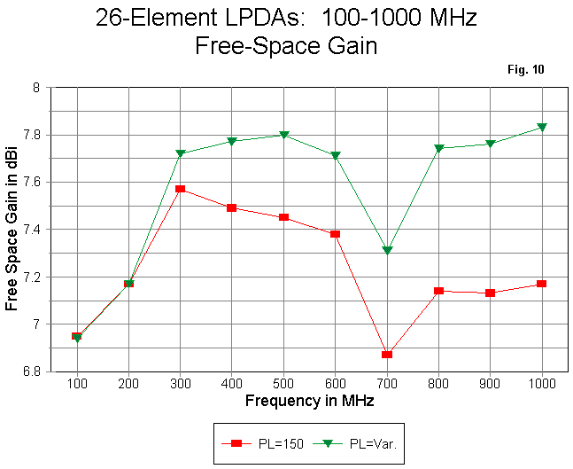
Tapering the phase-line characteristic impedance has one beneficial effect. It raises the array gain above 200 MHz by an average of 0.5 dB. The curves in Figure 10 compare the gain of the array designs. The general shape of the curve is preserved by the tapered phase line version, including the drop in the 700 MHz region. However, the overall level is higher except for the lowest frequencies in the span.
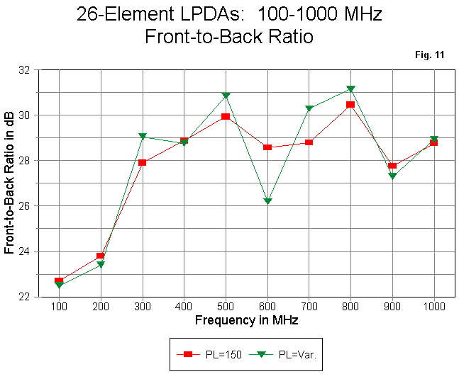
As seen in Figure 11, the front-to-back ratio is not harmed or enhanced by the phase line impedance tapering technique. The gain and front-to-back ratios, when examined in greater detail than used in the graphic shown here, exhibit periodic peaks and valleys. However, the gain and front-to-back for any given design do not show coincident peaks and valleys, and the exact frequencies of maximums and minimums will shift with minor design changes. Hence, the exact values in Figure 11 should not be interpreted as giving one version of the array a significant advantage over the other.
The higher gain of the tapered phase line impedance version of the array and its cost in terms of pattern behavior deserve a further note. A well-behaved azimuth pattern for an LPDA design has the appearance of a standard directional array pattern, for example, as might be produced by a Yagi. Figure 12 shows the free-space azimuth pattern at 200 MHz for the untapered version of the array as a simple demonstration of a well-behaved pattern.
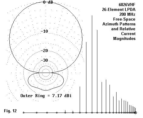
Observe the element with the highest relative current magnitude. Forward of that element, virtually all the elements are active. Behind the most active element, only two are very active (or have a significant current magnitude), and behind them, activity virtually disappears. This is the conditions for a very well-behaved pattern, such as the one in Figure 12.

Figure 13 shows the free-space azimuth pattern at 1000 MHz of the tapered phase line version of the model in order to demonstrate how far from well-behaved the patterns might go. To a lesser degree, the patterns at 900 and 1000 MHz of the constant impedance phase line model show some elements of the pattern distortion. However, in the tapered phase line model, the distortions appear at much lower frequencies. The degree of distortion is proportional in the main to the rising frequency.
The forward lobe shows the development of small side lobes. As well, the main portion of the forward lobe has lost its smooth oval and has taken on the appearance of a common garden trowel. The rear lobes have spread so that they are down from the main lobe by only about 17.5 dB at their peaks. Additionally, they show considerable ripple in their outline.
The graph of the relative current magnitude on the elements provides the reason why the pattern has grown distorted. Behind the most active element, there is considerable activity on a number of elements, although the current level decreases smoothly. However, there is also a region of increased current magnitude, indicating harmonic activity of the affected elements. In the main, it is this activity that yields the pattern distortion.

Figure 14 compares the free-space azimuth patterns of the two versions of the LPDA at 600 MHz. In this mid-passband region, the fixed impedance model shows greater pattern control, even though there are hints of potential irregularities compared to the well-behaved pattern of Figure 12. The tapered impedance model shows incipient secondary forward lobes and a greater ripple to the rear lobes than the fixed impedance version.
Carried to high levels of current, relative to the most active element, active elements behind the most active element would yield a potential weakness that might go so far as to produce a pattern reversal and an unusable feedpoint impedance. However, in the present designs, these consequences have been avoided. Still, an important user question remains.
Just how much pattern distortion is acceptable for an LPDA design? There is no simple answer to this question, since it necessarily involves goals and specifications brought to the antenna design be the user. For general utility purposes, the pattern distortion shown in Figure 13 might well be considered to be well within needs. For other purposes, the most well-behaved pattern achievable might be required. For utility purposes, either version of the 26-element LPDA shown here would be serviceable, with the final selection perhaps dictated by the desired feedpoint impedance.
There is a considerable difference between the 12-element sample models that were rejected and the 26-element models that proved to be reasonably successful. How many fewer elements than 26 might one use and obtain the necessary performance in terms of gain, an absence of weaknesses, and an acceptable SWR curve across the passband? There is, once more, no simple answer to the question. Each trial design may alter the value of Tau and Sigma, the total boom length, and the low and high frequencies used in the design exercise. For lower values of Tau, a lower minimum frequency should be used to ensure adequate gain near 100 MHz. As well, altering the length and spacing of the longest elements in accord with circularizing techniques may be useful in increasing low-end gain. If high end gain tapers off too badly, the design may use a higher maximum frequency or also employ circularizing techniques to adjust the most forward elements with respect to length and spacing.
When we combine the variables of both basic design and useful modifications, a general answer to the question of how few elements we may use and still achieve a desired level of performance becomes impossible. The examples of LPDA design given here represent but two of many possibilities. However, they do illustrate well the general guidance of using a long enough boom and using enough elements to ensure that we get the job done.
Originally posted on the AntennaX Online Magazine by L. B. Cebik, W4RNL
Last Updated : 6th June 2024
